As we saw in a previous article, perovskite-based photovoltaic devices have recently become one of the most active fields in solar cell research due to their low manufacturing cost and high efficiency when converting solar energy into electrical energy. It is also considered a material with great potential due to its superiority (compared to other materials), which may lead it to replace or complement silicon, the prevailing material in the field to date.
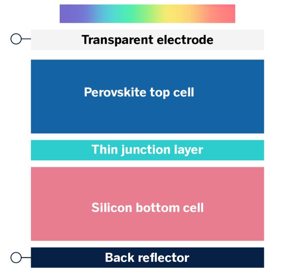
Schematic idea of what a perovskite and silicon tandem solar cell is: the higher energy photons are absorbed by the perovskite cell, which is located at the top of the structure, while the lower energy photons are absorbed by the silicon cell, which is located at the bottom. With the synergy of the two cells, the whole can overcome the 30% efficiency barrier, obtaining “the best of both worlds”
THE TANDEM DEVICE
The installation of photovoltaic modules has increased steadily over the last few decades. This is thanks to numerous stimulus programs implemented by the major industrialized countries, which has made photovoltaic solar energy the fastest growing renewable source of all power generation technologies. However, only 3.6% of electricity was produced worldwide from photovoltaics by the end of last year. To reach the objectives set out in the Paris Climate Agreement in 2015 to keep the pace of global average temperature rise below 2°C, it is imperative to use significantly more photovoltaic solar energy (and renewables in general) as methods of electricity generation. Therefore, it is of crucial importance to further accelerate the global installation of photovoltaic modules and the main tool to achieve success is to reduce what is called in the specific jargon, the Levelized Cost Of Energy, hereinafter referred to as LCOE).
At present, the dominant technology in the photovoltaic market is the homo-junction silicon solar cell (95% of the market) in all its variants, cells that are inherently limited in their efficiency of converting solar energy into electrical energy, as the value of that factor in these cells has only increased from 24.2% in 1990 to 26.7% as of today. This respresents a progression of just 2.5% in more than 30 years, indicating that silicon technology has already reached a high degree of maturity, with little room for improvement as a result. As I reported in a previous article, to raise these efficiency values significantly, one must combine different semiconductor materials to make solar cells with stacked structures on top of each other, generically called tandem devices, by intimately joining two solar cells of different materials that absorb different regions of the solar spectrum. This technological strategy allos us to increase the conversion efficiency to values clearly superior to those obtained with each cell working individually.
Given that tandem cells do not involve additional costs relating to increased area, these high-efficiency devices may be one of the best options available today to reduce LCOE in the future. This would require, however, for the gain in conversion efficiency to be such that it offsets the additional manufacturing costs. As a result, the photovoltaic industry has been searching for years for new candidate solar cells that are cost-effective and efficient for integration into tandem structures at costs competitive with today’s solar watt prices.
SILICON-PEROVSKITE TANDEM SOLAR CELLS
As we saw in a previous article, the materials known generically as perovskites absorb solar radiation very efficiently, which makes them ideal candidates for making efficient solar cells. Since the publication of the first solar cell based on these perovskites in 2009, these materials have become the hottest research topic in the the hottest research topic in the field of solar photovoltaics. At present, these devices meet the requirement of having perfect “partners” to fabricate two-junction tandem structures with semiconductors whose technologies are already very mature, such as silicon or CuInGaSe2 (CIGS). Briefly, these requirements are as follows:
i) Absorption of the solar spectrum complements that of the “partner”. That is, the perovskite cell absorbs the short wavelengths (high energies) of the spectrum while Si or CIGS absorbs the long wavelengths (lower energies).
(ii) High single cell conversion efficiency
iii) Ease of processing
(iv) A key factor: compatibility of the tandem device process with commercial silicon and CIGS technologies.
- i) Absorption of the solar spectrum complements that of the “partner”. That is, the perovskite cell absorbs the short wavelengths (high energies) of the spectrum while Si or CIGS absorbs the long wavelengths (lower energies).
(ii) High single cell conversion efficiency
iii) Ease of processing
(iv) A key factor: compatibility of the tandem device process with commercial silicon and CIGS technologies.
Illustrating the concept of what a silicon-perovskite tandem solar cell is
 Illustrating the concept of what a silicon-perovskite tandem solar cell is (left) and the areas of the solar spectrum absorbed by each individual cell (right)
All these technologies, which are still evolving, already allow conversion efficiencies higher than those of the best single-junction cells based on either partner, silicon or CIGS. This potential has been recognized not only by several universities and research institutes around the world, but also by several start-ups that will commercially exploit these devices in the near future, such as Oxford PV, Swift Solar and Tandem PV.
The following diagram schematically illustrates recent improvements and potential projections for the efficiency improvement of single junctions of silicon, CIGS and perovskite, displaying both laboratory and industrial scale results. While improvements in conversion efficiency are to be expected in all three individual technologies in the coming years, single junctions are not likely to exceed the practical limit of ~ 27% (and slightly lower in modules). This has triggered a great interest in tandem technology, which has already proven to be able to overcome this practical single-junction limit; since very recently an efficiency of a silicon-perovskite tandem cell above 30%. has been confirmed. Indeed, the first results of three-junction devices, with even greater potential, have already been published:
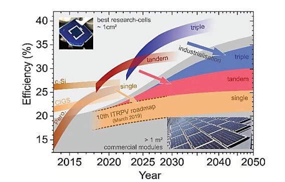
Possible efficiency improvement scenarios for photovoltaic devices based on silicon, CIGS and perovskites, in single, tandem and triple-junction cells.
The manufacturing routes for this new class of devices are reasonably inexpensive and tandem solar cells could be produced at low cost in the near future.
UNRESOLVED ISSUES
In addition to long-term stability, one of the problems that to be resolved is how to “place” the perovskite cell on the silicon cell, a matter that has not yet fully been resolved. It should be noted that the silicon on which the members of the perovskite solar cell are to be placed is not flat but has the rough appearance shown in the image:
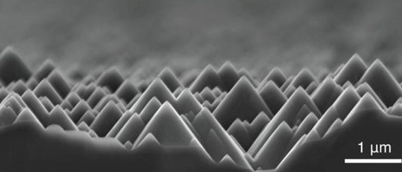
Silicon textured surface used in solar cells observed under the electron microscope. The surface has an irregular structure, made up of “pyramids”, the purpose of which is to increase light absorption
Early efforts to deposit perovskites on top of silicon “pyramids” quickly revealed a number of obstacles: some pyramids were not covered, current paths formed that caused short circuits, and in general, there was little control over the thickness of the perovskite layer. Of the many solutions being tested, scientists at the Helmholtz-Zentrum in Berlin have developed methods whose detail is far beyond the scope of this article, but which make it possible, in the words of one of the group’s scientists, “to prepare the perfect bed, so to speak, on which the perovskite lies”. The result is shown in the following image, which shows a cross section of one of these pyramids on top of which the perovskite cell has been deposited, with an excellent silicon coating:

Left: cross-section of the structure of a tandem cell made of silicon and perovskite. Right: electron microscopy image of the structure on the left, where we can perfectly see one of the silicon pyramids coated with the various layers that make up the perovskite cell. The scale of the image is detailed in the lower right corner
The field of silicon-perovskite tandem solar cells is currently the most active in the search for higher efficiencies. The value of 30% is is already a reality in the laboratory and the first modules based on this technology are about to go on the market. If developments continue at the current pace, we may see a photovoltaic market in which this technology will have a very significant share in the next few years.
Ignacio Mártil
Professor of Electronics at the Complutense University of Madrid and member of the Spanish Royal Society of Physics
Author of the book Energía solar: De la utopía a la esperanza (Análisis y crítica)
Comments on this publication