In 1965, Gordon Moore, co-founder of Fairchild Semiconductor, was asked by Electronics magazine to speculate on the future of transistor integrated circuits (IC), then the new technological revolution. In his article, Moore noted that the number of transistors per IC had doubled every year over the previous five years, which led him to predict that the same would happen in the following decade. In 1975, he updated his forecast: twice as many transistors per IC every two years. For half a century, Moore’s prediction has been law. Today, however, the end of Moore’s law is being proclaimed. But is it true?
The transistor, a kind of tiny switch controlled by electricity, was developed in 1947 by Bell Laboratories engineers John Bardeen, Walter Brattain and William Shockley. This advance replaced the bulky vacuum tube, which at the time was the option for amplifying the telephone signal along its path. In 1959, Mohamed Atalla and Dawon Kahng, also from Bell, invented the type of transistor that would be used for decades: MOSFET (Metal Oxide Semiconductor Field Effect Transistor).

The first MOSFET measured 20 microns in the parameter taken as a reference, the length of the Gate, the channel through which the electrons move from the Source to the Drain. But soon this size began to shrink. In 1987 it dropped to 0.8 microns, 800 nanometres (nm), and continued to fall in the following decades, until in 2012 the node —or successive generation in the development of these technologies— reached 22 nm. The smaller the size, the greater the number of transistors per microchip surface.
The limits of miniaturization
Each successive node has been reached in accordance with Moore’s law, which guided the construction of the International Technology Roadmap for Semiconductors (ITRS), the industry-sponsored roadmap with which companies improved their products while maintaining economic profitability. As Tom Conte, a computer scientist at Georgia Tech and former president of the Computer Society at the Institute of Electrical and Electronics Engineers (IEEE), told OpenMind, “Moore’s Law isn’t about the doubling of transistors per surface area; if you go back to Moore’s original article, it’s about the economics of the semiconductor industry. Putting it plainly, if you pay $1 for 1000 transistors today, you will pay $0.50 for 1000 transistors x years from today.”
But now in this century, Moore’s Law began to falter, as the engineer himself admitted in 2015. On the one hand, the miniaturization of MOSFET had a physical limit, while on the other hand, the benefits of reduction were also limited. “Sadly, the time when our chips were doubling in performance every couple of years has now come and gone,” Neil Thompson of the Massachusetts Institute of Technology (MIT) and an expert in digital economics told OpenMind. “Since the mid-2000s, one of the principal benefits from shrinking transistors, being able to run them faster, disappeared and with it many of the benefits that we had grown accustomed to getting. The second major benefit, getting more transistors, is now also at risk and is likely to slowly fade away as the engineering challenges and economics of chip production worsen.”
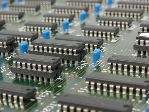
And yet, the specialist media keep reporting the new nodes being reached: 14 nm in 2014, 10 nm in 2016 and 7 nm in 2018, which was declared as the unbreakable physical limit. But in 2019, the first 5 nm transistors were manufactured, and 3 nm ones have been announced. Intel, the industry giant co-founded by Moore, has launched a bid for 1.4 nm in ten years.
However, it should be clarified that in nodes below 22 nm, “the node number no longer corresponds to any specific physical dimension,” Ignacio Mártil de la Plaza, Professor of Electronics at the Complutense University of Madrid and author of the book Microelectrónica: La historia de la mayor revolución silenciosa del siglo XX (Microelectronics: The history of the greatest silent revolution of the 20th century) (Ediciones Complutense, 2018), tells OpenMind. The reason is that the configuration of transistors has changed, so the advertised nodes are now “basically propaganda; in the fiercely competitive market of chip manufacturers, no one can hope to sell a product if it is not sold with some advantage that can be easily advertised,” says Mártil de la Plaza. According to what Erik DeBenedictis of Sandia National Laboratories and co-chair of the IEEE Rebooting Computing initiative explained to OpenMind, instead of geometric scaling based on reducing the same type of transistor, today we “seek to create an equivalent linewidth for other non-geometrical changes in semiconductors.”
The way to go is up and the move to 3D
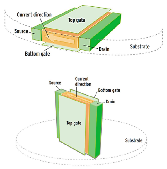
Thus, the roadmap established by Moore’s law has been abandoned, and in 2016 the ITRS was no longer updated. Today, companies are looking for new ways to move forward and continue to stand out from their competitors. The latest developments present new options: the first of which is vertical transistors. “This is what gave us high-rise cities like New York,” says Conte, also co-chairman of Rebooting Computing. “Manhattan is land locked. If you want to be in Manhattan, the only way to go is up!”
“Since 2012, the big manufacturers in the industry (Samsung, Intel, TSMC and GlobalFoundries) no longer make MOSFET technology chips, but rather FinFET, a vertical, not horizontal device,” says Mártil de la Plaza. In FinFETs, not only is the meaning of the length of the gate lost, but Moore’s Law is diluted: “It was enunciated in a 2D world,” says the professor. The move to 3D is one of the paths marked out by Rebooting Computing’s International Roadmap for Devices and Systems (IRDS), which has taken over from the ITRS.
But experts warn that 3D integration is only one of the paths on that roadmap on which we are already travelling. Other paths explore new materials, architectures or specialization, “building chips that do fewer functions but do them better,” Thompson says, citing examples such as Graphics Processing Units (GPUs) or Artificial Intelligence chips. “The change is no longer a direct improvement in one aspect of performance, but improvements in a more diverse set of metrics,” summarizes DeBenedictis. With Moore’s Law gone, the current roadmap is no longer one-dimensional, and for Conte, “the winner will be diversity in implementation.”
But in addition to all this, there is one more question: will the progress of microelectronics be compatible with a world that is increasingly aware of environmental issues? “The microelectronics industry is anything but sustainable if you look at the entire production cycle, from raw material extraction to obtaining the IC,” says Mártil de la Plaza. According to the expert, the manufacturing processes are scrupulously respectful of the environment, but the materials are another matter: “Vanadium, niobium, titanium, tungsten, germanium and a long etcetera. If we look at where the sources of these materials are and what technologies are used to extract them, process them and, crucially, purify them, it is very disappointing.”
Javier Yanes
@yanes68
Comments on this publication